What is a Test Point?
Test Point – Location Where Test Is Conducted – Quality Assurance (PCB/Electronics)
Definition and Technical Nature
A test point in PCBs and electronics is a deliberately designed and marked location, such as a small metal pad, plated through-hole, loop, or post, on a printed circuit board (PCB) that provides direct electrical access to a specific signal or net within the circuit. These features facilitate attachment of test probes, whether manually (oscilloscope, multimeter) or via automated equipment, at various stages of development, manufacturing, and quality assurance.
Test points are typically made from highly conductive metals like phosphor bronze or silver-plated copper, ensuring excellent electrical contact and mechanical durability. Their physical form depends on the testing method: low-profile pads for surface mount, loops or posts for through-hole or J-hook probes, and controlled impedance structures for high-frequency measurements.
In PCB design software (such as Altium, Cadence Allegro), test points are flagged in schematic and layout, with coordinates and net associations exported for fixture programming and test automation.
Where Used:
Test points are fundamental in consumer electronics, automotive, aerospace, industrial control, telecommunications, and medical devices, anywhere PCBs are manufactured and maintained.
Functional Purpose and Application
The main role of a test point is to provide a reliable, accessible interface for monitoring, measuring, or injecting signals into a circuit without disturbing normal operation. Test points support:
- Manufacturing Testing: Automated systems (In-Circuit Testers, Flying Probe Testers) use test points to verify solder joints, component placement, and detect assembly errors. This enables rapid fault detection and process yield analysis.
- Quality Assurance & Compliance: Systematic testing against regulatory standards (EMC, functional safety like ISO 26262, IEC 60601) is enabled by accessible test points, supporting traceable measurement and auditing.
- Debugging & Field Service: Engineers and technicians use test points for fault diagnosis, waveform capture, and real-time monitoring, especially in complex, multi-layer PCBs.
- Programming & Calibration: Test points can serve as access for factory programming (e.g., SWD/JTAG for microcontrollers) or for calibrating analog/RF circuits.
- Prototyping & Design Validation: During hardware iteration, test points permit quick validation, power measurement, and signal integrity analysis without destructive modifications.
Well-placed test points are a hallmark of design-for-test (DFT) practices, ensuring efficient validation and rapid field diagnosis.
Types of Test Points
| Type | Description | Application Scenario |
|---|---|---|
| Manual Probe Point | Large pads, loops, or posts for direct contact by handheld probes. | Debugging, field servicing, R&D |
| Automated Test Point | Small pads/vias for contact by automated systems (ICT, flying probe). | Production, automated QA |
| Socket/Pin Test Point | Through-hole or SMT sockets/pins for repeated connections, e.g., programming or calibration. | Programming, calibration, rework |
| Connector Test Point | Larger connectors for bulk signal or power testing. | Power testing, multi-signal capture |
| Specialized/Impedance TP | Structures for controlled impedance or RF measurement (TDR, S-parameter coupons). | RF, high-speed digital, signal integrity |
| Integrated/Hidden Test Point | Pads/vias under components or in dense areas, sometimes only exposed during specific assembly steps. | Compact designs, HDI, BGA escape |
Manual probe points are marked on silkscreen (TP1, TP2). Automated points are optimized for fixture compatibility and minimal space. In dense designs, microvias or small SMT pads are used, requiring fine-pitch probes.
Test Point Placement and Design Considerations
Size and Shape:
Manual probe pads: typically 0.050" (1.27 mm) diameter, minimum 0.035" (0.89 mm) for compact designs. Square pads can distinguish test points from round component pads. Posts or loops are used for robust, repeated probing.
Spacing:
Recommended: 0.100" (2.54 mm) center-to-center, absolute minimum: 0.050" (1.27 mm) for high-density boards. Distance to component edge or PCB edge: ≥0.125" (3.18 mm) to prevent probe slippage or fixture misalignment.
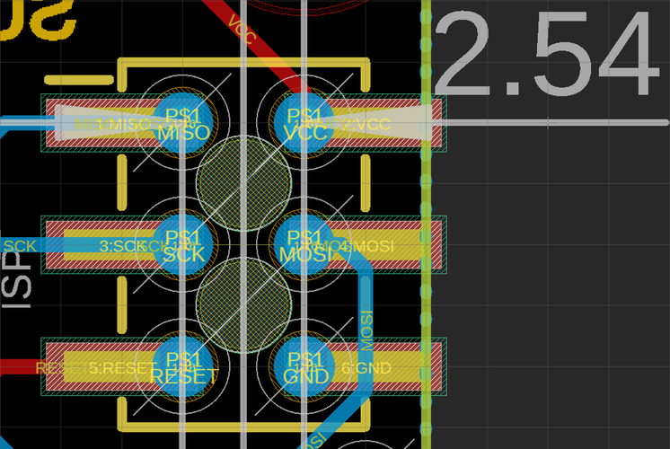
Proper spacing and placement of test points prevent mechanical interference and enable simultaneous probing.
Board Side and Distribution:
Placing all test points on one side (usually the bottom) simplifies fixture design and reduces handling. Even distribution prevents board flexing and ensures uniform fixture pressure.
Accessibility:
Test points must not be blocked by tall components. In dense layouts, place them in clear regions or at the board perimeter.
Labeling and Documentation:
Mark test points with clear silkscreen labels and maintain consistent naming in all documentation and design files.
CAD Integration:
Modern PCB tools automate test point assignment and rule-checking, ensuring compliance with design and manufacturing constraints.
Test Point Implementation in Manufacturing and QA
Automated Test Methods
In-Circuit Testing (ICT):
A bed-of-nails fixture with spring-loaded pins contacts all test points simultaneously for rapid, parallel measurement of continuity, resistance, and basic function. High setup cost, but justified for high-volume production.
Flying Probe Testing (FPT):
Robotic probes sequentially contact test points. Slower than ICT, but flexible and cost-effective for prototypes or small batches.
| Feature | In-Circuit Testing (ICT) | Flying Probe Testing (FPT) |
|---|---|---|
| Connections | Parallel | Sequential |
| Test Speed | Very fast | Slower |
| Setup Cost | High (custom fixture) | Low (no fixture) |
| Change Management | Expensive, slow | Fast, flexible |
| Best Use | High-volume production | Prototyping, small runs |
Both methods require validated test point layouts for fixture/probe reach. Automated Optical Inspection (AOI) may use test points as fiducials.
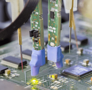
Automated flying probe system performing sequential test point verification.
Challenges in Test Point Design
- Space Constraints: Miniaturized and HDI designs limit space for test points. Solutions include microvias or using existing pads/vias.
- Component Interference: Tall or dense components can block probe access. Plan component and test point placement together.
- Signal Integrity Risks: Test points add parasitics, potentially degrading high-speed or sensitive analog signals. Use controlled impedance where necessary.
- Mechanical/Thermal Stress: Excess fixture pressure can damage pads or flex boards. Distribute test points evenly.
- Manufacturing Variability: Tolerances in PCB fabrication can affect probe alignment. Account for pad and hole size variations.
Best Practices for Test Point Integration
- Prioritize Critical Nets: Assign test points to power, ground, and key functional nets first.
- Maintain Spacing/Clearance: Follow recommended spacing for probe and fixture compatibility.
- Consistent Labeling: Standardize naming (TP1, TP2, etc.) in layout and documentation.
- Automate Assignment: Use CAD tools to auto-select and manage test point locations.
- Plan Fixture Needs Early: Collaborate with test/fixture engineers during layout.
- Design for Maintainability: Ensure accessibility after coating/enclosure, use headers if needed.
- Review Signal Integrity: Simulate effects on high-speed/sensitive nets.
- Document for Traceability: Export coordinates/netlists for QA and manufacturing.
Industry Standards and Guidelines
IPC-2221 is the key standard for test point design, covering physical dimensions, spacing, and marking. Many OEMs/EMS providers have proprietary DFT checklists, sometimes stricter than IPC guidelines. Trends include intelligent CAD algorithms for automated placement and 3D-printed fixtures for rapid prototyping.
Practical Example
For a medical device PCB with a microcontroller, test points are assigned to VCC, GND, peripherals, and programming nets. During assembly, an ICT fixture checks soldering and placement. In the field, service techs diagnose issues using labeled test points, ensuring safety and compliance with ISO 13485.
Summary Table: Test Point Design Recommendations
| Parameter | Recommended Value | Absolute Minimum |
|---|---|---|
| Test Point Pad Size | 0.050" (1.27 mm) | 0.035" (0.89 mm) |
| Test Point Spacing (center-to-center) | 0.100" (2.54 mm) | 0.050" (1.27 mm) |
| Test Point to Component Edge | 0.100" (2.54 mm) | 0.050" (1.27 mm) |
| Test Point to Board Edge | 0.125" (3.18 mm) | 0.100" (2.54 mm) |
Conclusion
Test points are essential for efficient manufacturing, QA, and field maintenance of electronic products. Thoughtful test point planning ensures fast validation, easier diagnostics, and robust, maintainable designs. Integrate test point strategy early in PCB layout and adhere to standards like IPC-2221 for reliable, testable electronics.
References
- ELEPCB: The Best Guide of PCB Test Points
- MOKOTECHNOLOGY: Definition, Importance and Application of PCB Test Point
- PCBTrace: PCB Test Points: A Complete Guide to Efficient Electronics Testing
- IPC-2221: Generic Standard on Printed Board Design
- Cadence: Circuit Board Testing for Manufacturing Verification
- 911EDA: Test Points in PCB Design
- FixturFab: Test Point Spacing
This glossary entry explains test points in PCBs and electronics, ensuring engineers and quality professionals can design, implement, and use them for efficient and reliable testing across the product lifecycle.
Frequently Asked Questions
- Can I use existing component pads or vias as test points?
- Yes, if they are accessible and meet the required size and spacing for test probes, existing pads or vias can be designated as test points. This approach helps save PCB space and is often flagged in CAD tools for efficient test planning.
- What size and spacing should test points have?
- A recommended pad diameter is 0.050" (1.27 mm) with a minimum center-to-center spacing of 0.100" (2.54 mm). For high-density boards, absolute minimums are 0.035" (0.89 mm) diameter and 0.050" (1.27 mm) spacing.
- Do test points affect signal integrity?
- Test points add small amounts of capacitance and inductance, which can impact high-speed or sensitive analog signals. For such nets, simulate and review the effects, and use controlled impedance structures if needed.
- Are test points needed for every net?
- Ideally, every net should be accessible for in-circuit testing, but at minimum, assign test points to power, ground, and all critical or high-risk nets for effective QA and diagnostics.
- How do I document test points?
- Label test points clearly in silkscreen (TP1, TP2, etc.) and ensure consistent naming in the schematic, layout, and manufacturing/test documentation. Export coordinates and netlists for manufacturing and QA teams.
This is a reference entry. TarmacView provides drone inspection services and doesn't sell the equipment or materials described in this glossary.